#
はじめに
最近、低レイヤーやりたい!ということで論理回路をやろう!となって、turing completeというゲームを始めました。
でも単に解いただけだとつまらないので、実世界に応用したらめっちゃ面白いと思い、icarus verilogというシミュレーションソフトを使い、system verilogを書くことにしました。
今回の取り組みはturing completeの再現なので、verilogの組み込み演算子はNANDゲートを作るときのみという縛りをかけています。(どうしてものときは少し許容しています。)
verilogを書くのは本当に初めてなので、雰囲気で書いています…
本当の最初の取っ掛かりの部分はこのブログを参考にさせていただきました。
#
基本回路
#
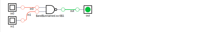
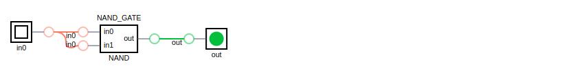
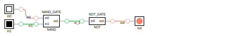
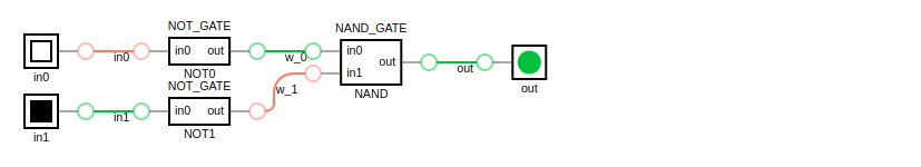
NAND回路
1
2
3
4
5
6
7
|
module NAND_GATE(
     input wire       in0,
     input wire       in1,
     output wire       out
);
    assign out = ~ ( in0 & in1 );
endmodule
|
#
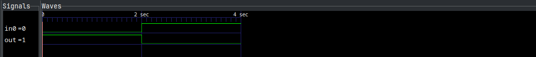
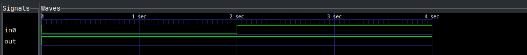
NOT回路
 1
 2
 3
 4
 5
 6
 7
 8
 9
10
|
module NOT_GATE(
     input wire       in0,
     output wire       out
);
    NAND_GATE NAND(
        .in0    (in0    ),
        .in1    (in0    ),
        .out    (out    )
    );
endmodule
|
#
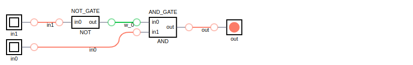
AND回路
 1
 2
 3
 4
 5
 6
 7
 8
 9
10
11
12
13
14
15
16
17
18
|
module AND_GATE(
     input wire       in0,
     input wire       in1,
     output wire       out
);
    wire w_1;
    NAND_GATE NAND(
        .in0    (in0    ),
        .in1    (in1    ),
        .out    (w_1    )
    );

    NOT_GATE NOT(
        .in0    (w_1    ),
        .out    (out    )
    );

endmodule
|
#
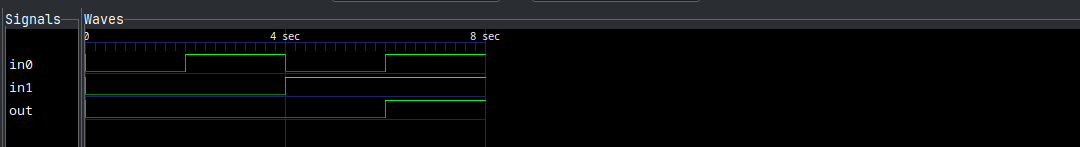
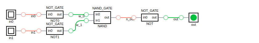
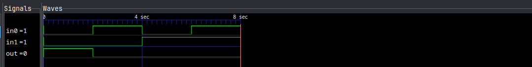
NOR回路
 1
 2
 3
 4
 5
 6
 7
 8
 9
10
11
12
13
14
15
16
17
18
19
20
21
22
23
24
25
26
|
module NOR_GATE(
     input wire       in0,
     input wire       in1,
     output wire       out
);
    wire w_0;
    wire w_1;
    wire n_out;
    NOT_GATE NOT0(
        .in0    (in0    ),
        .out    (w_0    )
    );
    NOT_GATE NOT1(
        .in0    (in1    ),
        .out    (w_1    )
    );
    NAND_GATE NAND(
        .in0    (w_0    ),
        .in1    (w_1    ),
        .out    (n_out    )
    );
    NOT_GATE NOT(
        .in0    (n_out    ),
        .out    (out    )
    );
endmodule
|
#
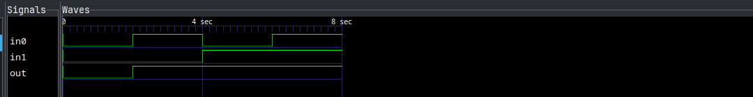
OR回路
 1
 2
 3
 4
 5
 6
 7
 8
 9
10
11
12
13
14
15
16
17
18
19
20
21
|
module OR_GATE(
     input wire       in0,
     input wire       in1,
     output wire       out
);
    wire w_0;
    wire w_1;
    NOT_GATE NOT0(
        .in0    (in0    ),
        .out    (w_0    )
    );
    NOT_GATE NOT1(
        .in0    (in1    ),
        .out    (w_1    )
    );
    NAND_GATE NAND(
        .in0    (w_0    ),
        .in1    (w_1    ),
        .out    (out    )
    );
endmodule
|
#
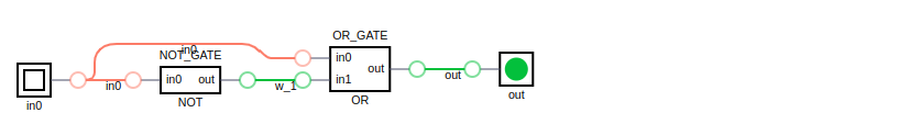
常時ON
 1
 2
 3
 4
 5
 6
 7
 8
 9
10
11
12
13
14
15
|
module ALWAYS_ON_GATE(
     input wire       in0,
     output wire       out
);
    wire w_1;
    NOT_GATE NOT(
        .in0    (in0    ),
        .out    (w_1    )
    );
    OR_GATE OR(
        .in0    (in0    ),
        .in1    (w_1    ),
        .out    (out    )
    );
endmodule
|
#
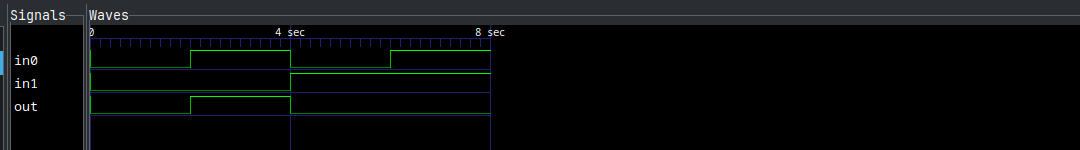
片方ONだと強制オフ(原文second tick)
 1
 2
 3
 4
 5
 6
 7
 8
 9
10
11
12
13
14
15
16
17
|
module SECOND_TICK(
     input wire       in0,
     input wire       in1,
     output wire       out
);
    wire w_0;
    wire n_out;
    NOT_GATE NOT(
        .in0    (in1    ),
        .out    (w_0    )
    );
    AND_GATE AND(
        .in0    (w_0    ),
        .in1    (in0    ),
        .out    (out    )
    );
endmodule
|
#
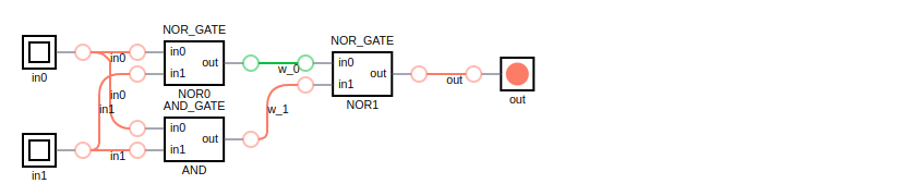
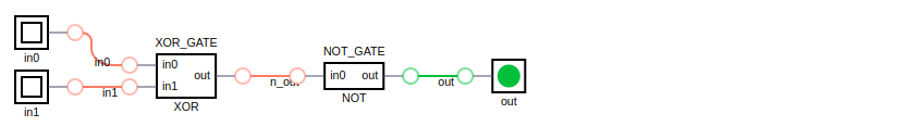
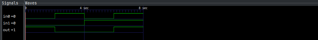
XOR回路
 1
 2
 3
 4
 5
 6
 7
 8
 9
10
11
12
13
14
15
16
17
18
19
20
21
22
23
24
25
26
|
module XOR_GATE(
     input wire       in0,
     input wire       in1,
     output wire       out
);
    wire w_0;
    wire w_1;

    NOR_GATE NOR0(
        .in0    (in0    ),
        .in1    (in1    ),
        .out    (w_0    )
    );

    AND_GATE AND(
        .in0    (in0    ),
        .in1    (in1    ),
        .out    (w_1    )
    );
    NOR_GATE NOR1(
        .in0    (w_0    ),
        .in1    (w_1    ),
        .out    (out    )
    );

endmodule
|
#
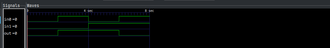
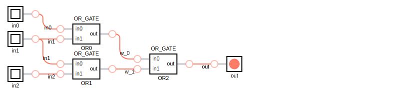
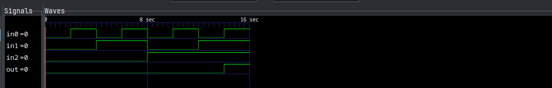
3入力OR回路
 1
 2
 3
 4
 5
 6
 7
 8
 9
10
11
12
13
14
15
16
17
18
19
20
21
22
23
24
25
26
27
|
module BIGGER_OR_GATE(
     input wire       in0,
     input wire       in1,
     input wire       in2,
     output wire       out
);
    wire w_0;
    wire w_1;

    OR_GATE OR0(
        .in0    (in0    ),
        .in1    (in1    ),
        .out    (w_0    )
    );

    OR_GATE OR1(
        .in0    (in1    ),
        .in1    (in2    ),
        .out    (w_1    )
    );
    OR_GATE OR2(
        .in0    (w_0    ),
        .in1    (w_1    ),
        .out    (out    )
    );

endmodule
|
#
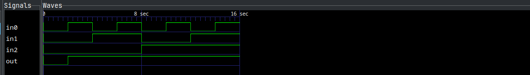
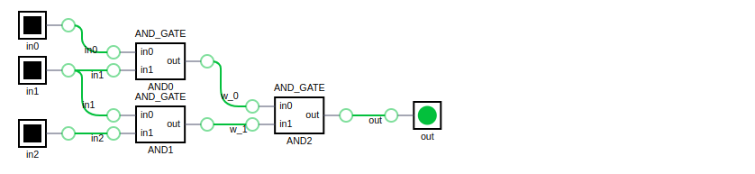
3入力AND回路
 1
 2
 3
 4
 5
 6
 7
 8
 9
10
11
12
13
14
15
16
17
18
19
20
21
22
23
24
25
26
27
28
|
module BIGGER_AND_GATE(
     input wire       in0,
     input wire       in1,
     input wire       in2,
     output wire       out
);
    wire w_0;
    wire w_1;

    AND_GATE AND0(
        .in0    (in0    ),
        .in1    (in1    ),
        .out    (w_0    )
    );

    AND_GATE AND1(
        .in0    (in1    ),
        .in1    (in2    ),
        .out    (w_1    )
    );
    AND_GATE AND2(
        .in0    (w_0    ),
        .in1    (w_1    ),
        .out    (out    )
    );


endmodule
|
#
XNOR回路
 1
 2
 3
 4
 5
 6
 7
 8
 9
10
11
12
13
14
15
16
|
module XNOR_GATE(
     input wire       in0,
     input wire       in1,
     output wire       out
);
    wire n_out;
    XOR_GATE XOR(
        .in0    (in0    ),
        .in1    (in1    ),
        .out    (n_out    )
    );
    NOT_GATE NOT(
        .in0    (n_out    ),
        .out    (out    )
    );
endmodule
|
#
まとめ
ここまでで基本回路編をすべて実装できました!
次はmemory編とarithmetic編を書いていきます!!
verilogは書いていて楽しいです。